

 >
首页 > HTCZ > science space and highlighted projects > scientific innovation > world's top 500 R&D centers
>
首页 > HTCZ > science space and highlighted projects > scientific innovation > world's top 500 R&D centers
来源:HTCZ 发布时间:2023.09.15
大中小
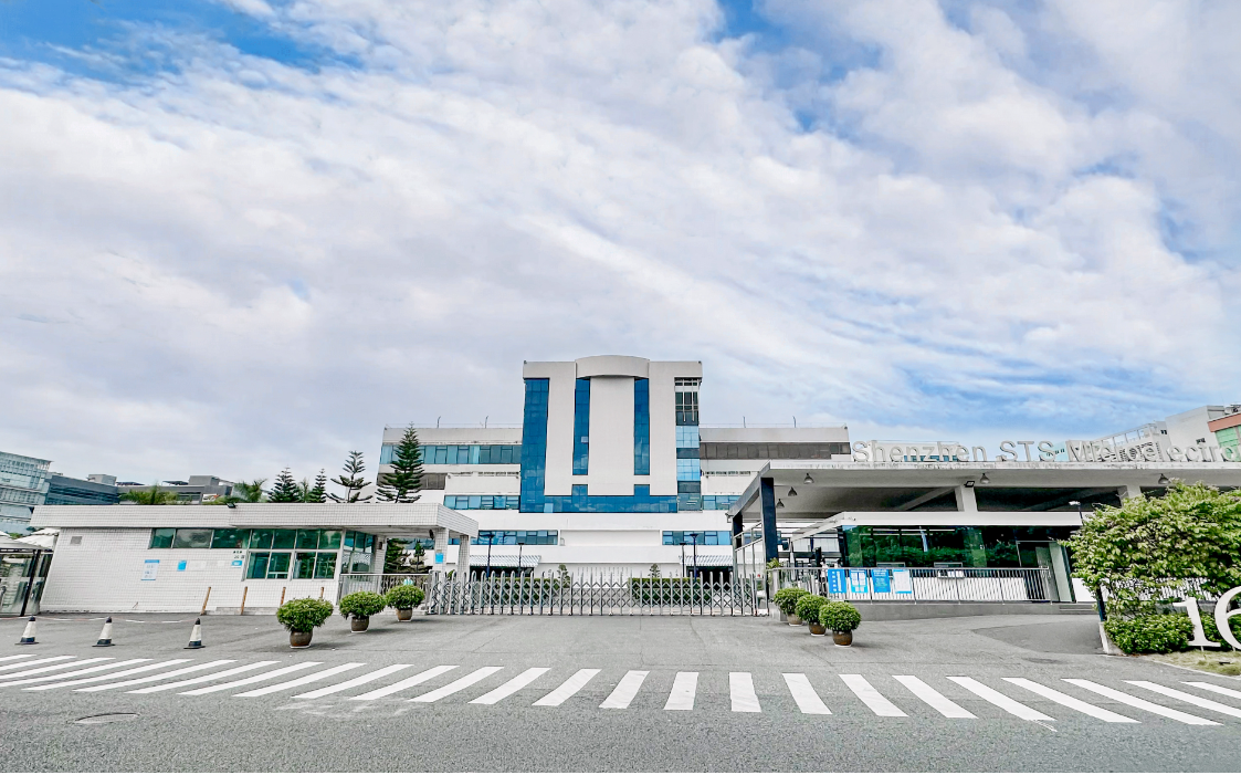
ST Global Packaging and Testing Innovation Center is sited in the "GBA Chip Valley" Core Startup Building. It is the only packaging and testing R&D center instituted by STMicroelectronics in the world. The planned facilities are the design failure analysis laboratory, reliability and materials laboratory, optical module packaging R&D laboratory, advanced power module packaging R&D laboratory, automation and robot R&D laboratory, and advanced power devices packaging R&D laboratory. This center has a professional R&D team that masters the cutting-edge technologies in the industry, that is capable of innovation and creation and that focuses on development of new products and application of scientific achievements, so as to provide technical support in solving the "bottleneck" problems in integrated circuit and facilitate development of high-end packaging and testing technology in the Guangdong-Hong Kong-Macao Greater Bay Area.